
Tata Electronics and ASML have signed a strategic partnership agreement tied to India’s first commercial front-end semiconductor fabrication plant, marking a significant step in the country’s effort to establish domestic chip manufacturing capacity.
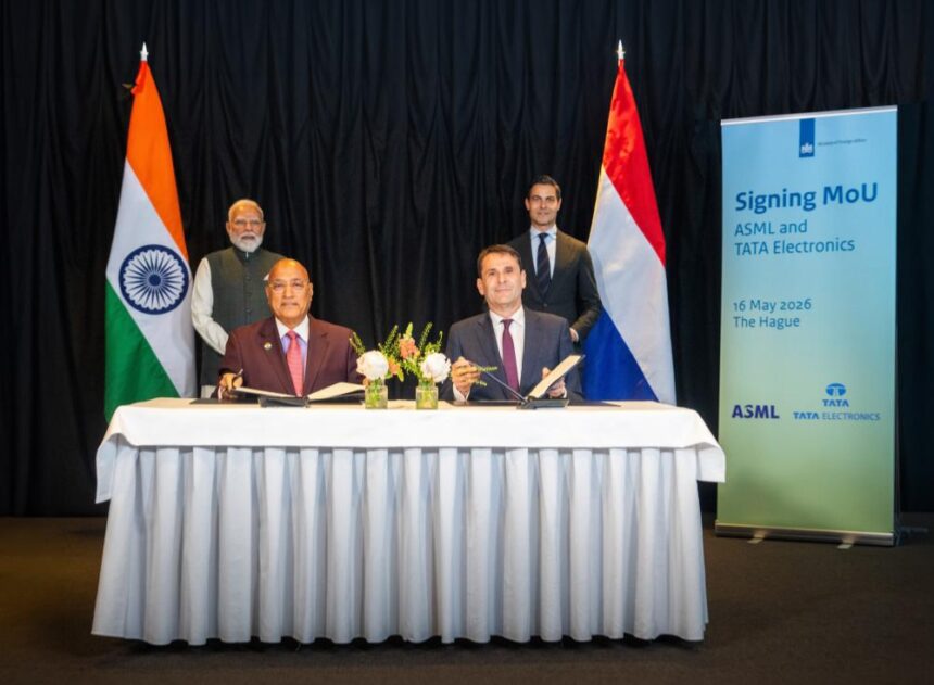
The memorandum of understanding was announced on May 16 during Indian Prime Minister Narendra Modi’s visit to the Netherlands. The agreement was signed in the presence of Modi and Dutch Prime Minister Dick Schoof, according to statements released by Tata Electronics and multiple international news reports.
The partnership centers on Tata Electronics’ planned semiconductor fabrication facility in Dholera, Gujarat. Under the agreement, ASML will provide lithography systems and related semiconductor manufacturing technologies for the project. The companies also said they will collaborate on workforce development, technical training, research initiatives, and supply-chain support.
In a statement published by Tata Electronics, the companies described the agreement as part of a broader effort to support the development of India’s semiconductor manufacturing ecosystem.
The Dholera facility has been widely described as India’s first commercial 300 mm wafer fabrication plant. The project is expected to manufacture semiconductors used in automotive systems, industrial equipment, mobile devices, and artificial intelligence-related applications.
Tata Electronics previously announced a partnership with Taiwan-based Powerchip Semiconductor Manufacturing Corporation (PSMC), which is providing process technology and operational support for the facility. The addition of ASML gives the project a critical equipment partner at a time when semiconductor manufacturing infrastructure has become increasingly difficult to secure globally.
ASML, headquartered in the Netherlands, is one of the most important suppliers in the semiconductor industry. The company produces lithography systems used to manufacture integrated circuits and supplies equipment to major global chipmakers including TSMC, Samsung, and Intel.
While neither company disclosed the exact systems that will be supplied to the Dholera fab, Tata Electronics has previously stated that the facility is expected to focus on mature process nodes including 28nm, 40nm, 55nm, 90nm, and 110nm technologies.
Those process technologies are commonly used in automotive electronics, power management chips, display drivers, industrial systems, and connectivity hardware. Industry analysts have noted that these categories remain strategically important because of strong global demand and recurring supply shortages in recent years.
According to reporting from Reuters, the Dholera project is estimated at roughly $11 billion in investment. The fab is expected to operate on 300 mm wafers, the standard size used in modern high-volume semiconductor manufacturing.
The agreement also reflects broader geopolitical and economic shifts in the semiconductor sector. Governments and technology companies across several regions have increased investment in domestic semiconductor production following supply-chain disruptions and rising concerns over concentration in global chip manufacturing.
India has accelerated its semiconductor ambitions through the country’s semiconductor incentive program, which includes financial support for fabrication plants, assembly facilities, and semiconductor packaging operations.
The Tata-ASML agreement comes as India seeks to move beyond semiconductor design and software engineering into large-scale manufacturing. India already has a strong presence in chip design services and engineering talent, but front-end wafer fabrication remains a new area for the country.
The workforce development component of the agreement may prove particularly important for the long-term viability of the project. Semiconductor fabs require highly specialized engineers and technicians trained in lithography, contamination control, equipment maintenance, and yield management.
In their announcement, the companies said the partnership would include training and knowledge-sharing initiatives aimed at building local semiconductor expertise in India.
Several operational details about the Dholera fab remain undisclosed. Neither Tata Electronics nor ASML has publicly confirmed the delivery timeline for equipment, projected monthly wafer output, or the facility’s expected production start date.
The companies also did not announce any plans related to leading-edge semiconductor manufacturing. Current public information indicates that the facility will focus on mature-node production rather than advanced processes used for the latest high-performance computing chips.
Even so, the partnership is being viewed as a major milestone for India’s semiconductor manufacturing plans because it brings together three critical components required for a functioning fabrication ecosystem: capital investment from Tata Electronics, process expertise from PSMC, and manufacturing equipment from ASML.
The agreement also places the Dholera project among a growing number of semiconductor manufacturing initiatives outside traditional chipmaking hubs in East Asia.